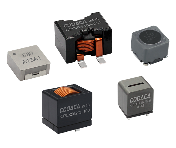
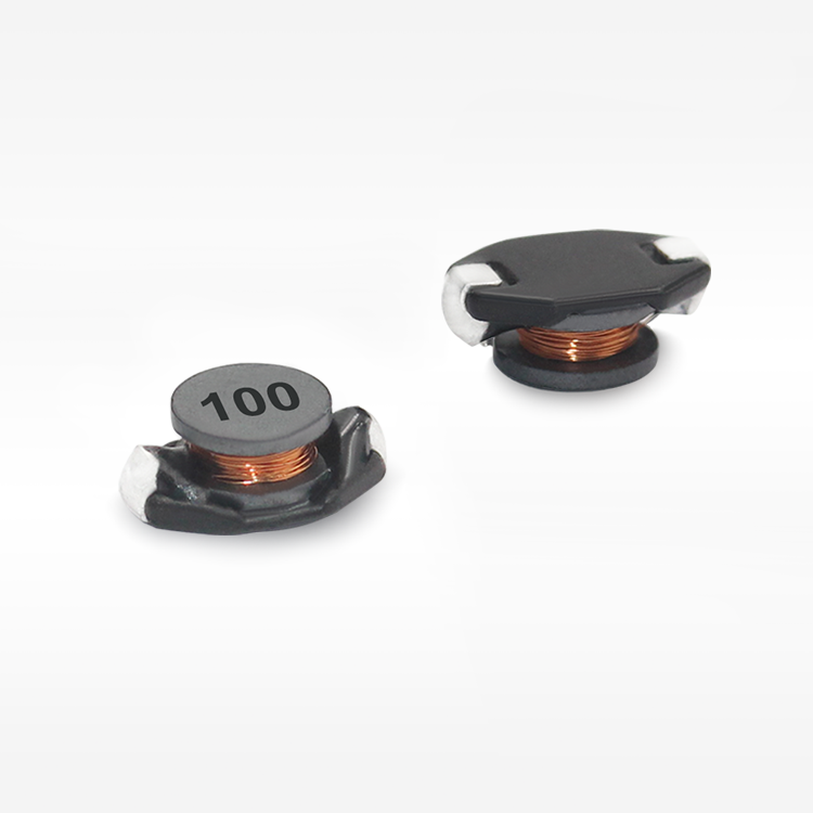
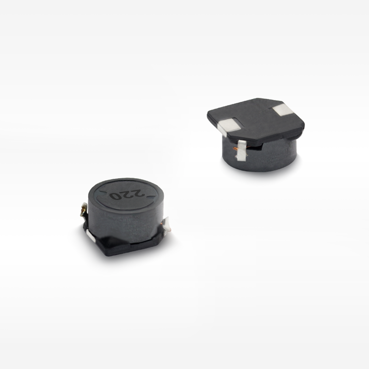
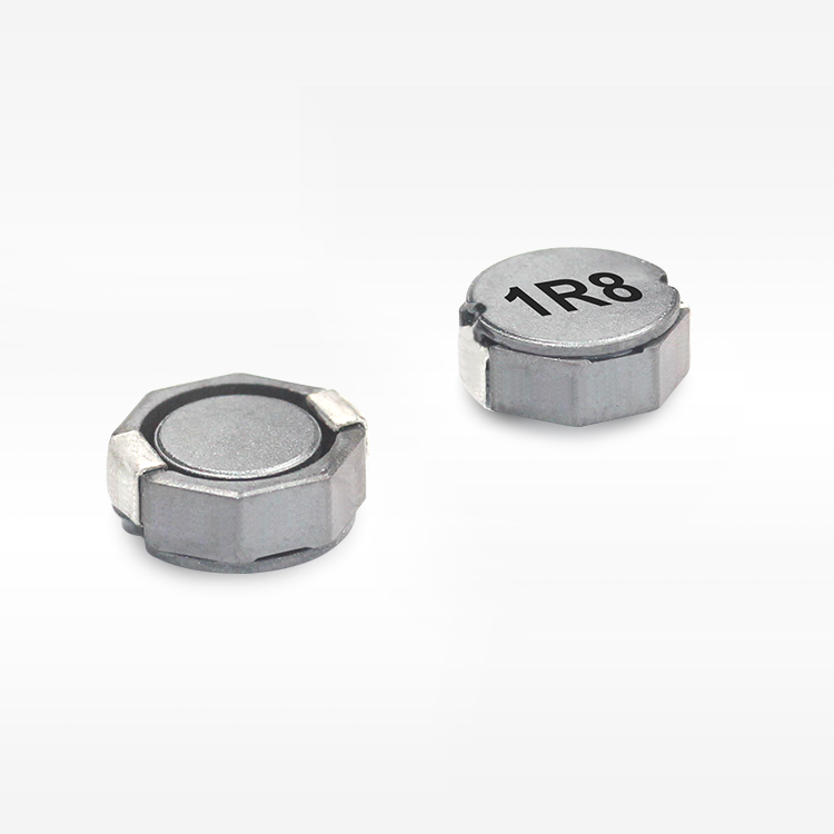
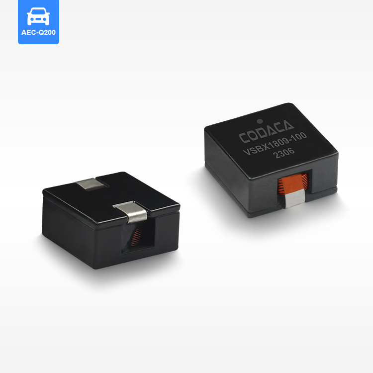
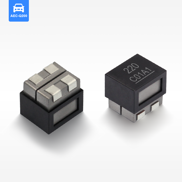
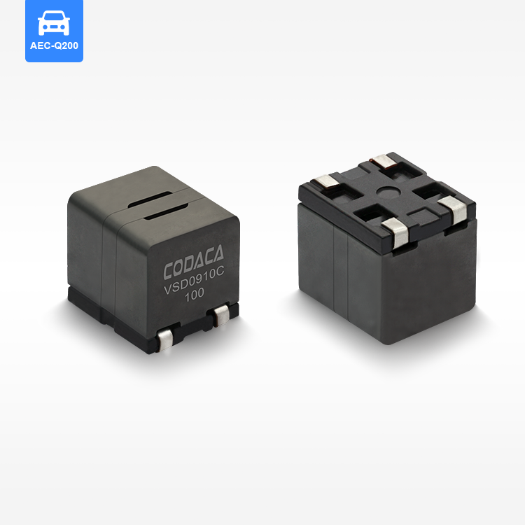
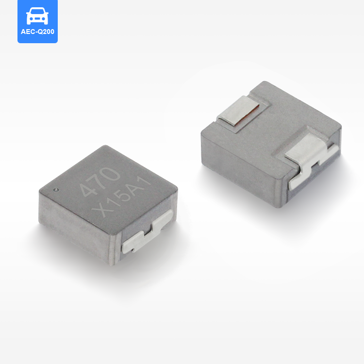
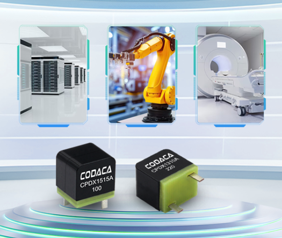
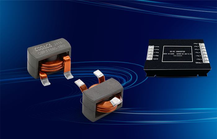
Shielded SMD Power Inductors - High Performance Magnetic Components for Power Management

All Categories

Get a Free Quote

Our representative will contact you soon.
Email
Name
Company Name
Message
0/1000

shielded smd power inductor

A shielded smd power inductor represents a critical component in modern electronic circuits, designed to store energy in magnetic fields while maintaining exceptional electromagnetic compatibility. These compact surface-mount devices combine advanced magnetic core materials with precision-engineered shielding to deliver superior performance in power management applications. The shielded smd power inductor features a closed magnetic core structure that significantly reduces electromagnetic interference (EMI) and minimizes flux leakage, making it ideal for high-density circuit boards where space constraints and signal integrity are paramount. The technological foundation of the shielded smd power inductor relies on ferrite or powder iron cores encased within a magnetic shield, creating a self-contained magnetic circuit that prevents interference with adjacent components. This design architecture enables higher inductance values in smaller footprints while maintaining stable electrical characteristics across varying temperatures and frequencies. Manufacturing processes for shielded smd power inductors involve precision winding techniques, automated assembly, and rigorous quality control measures to ensure consistent performance parameters. The primary functions include energy storage, current filtering, voltage regulation, and noise suppression in switching power supplies, DC-DC converters, and various power management circuits. Applications span across automotive electronics, telecommunications infrastructure, consumer electronics, industrial automation systems, and renewable energy equipment. The shielded smd power inductor excels in environments requiring high reliability, compact dimensions, and excellent thermal performance. Key technological features include low DC resistance for improved efficiency, high saturation current ratings for robust power handling, and superior temperature stability for consistent operation across wide environmental ranges. The magnetic shielding eliminates the need for additional spacing between components, enabling more compact PCB layouts and reducing overall system costs while maintaining optimal electromagnetic performance in sensitive electronic applications.

New Product Releases

The shielded smd power inductor offers numerous practical benefits that directly translate to improved product performance and reduced manufacturing costs for electronic device manufacturers. These components deliver exceptional electromagnetic interference suppression, eliminating the need for additional shielding measures that would otherwise increase board space requirements and assembly complexity. Manufacturers can achieve higher component density on printed circuit boards because the integrated magnetic shielding prevents coupling between adjacent inductors and sensitive analog circuits. This spatial efficiency reduces overall product dimensions and material costs while improving manufacturing yields. The shielded smd power inductor provides superior thermal management through optimized core materials and construction techniques that facilitate heat dissipation, resulting in longer component life and enhanced reliability under demanding operating conditions. Power conversion efficiency improves significantly due to reduced core losses and lower equivalent series resistance, which directly translates to extended battery life in portable devices and reduced energy consumption in larger systems. Installation becomes streamlined with automated pick-and-place assembly processes, as the shielded smd power inductor maintains consistent orientation and placement accuracy, reducing assembly time and labor costs. Quality control benefits from standardized testing procedures and predictable electrical characteristics that remain stable across production batches. The robust construction withstands mechanical stress from thermal cycling, vibration, and handling during manufacturing and field operation, minimizing warranty claims and field failures. Circuit designers appreciate the simplified design process enabled by comprehensive application data and simulation models that accelerate time-to-market for new products. Cost optimization occurs through reduced component count, simplified PCB layouts, and elimination of external shielding components. The shielded smd power inductor supports wide input voltage ranges and various switching frequencies, providing design flexibility for multiple product variants using common components. Environmental compliance becomes easier with RoHS-compliant materials and manufacturing processes that meet international regulatory standards without performance compromises or additional certification requirements.

Tips And Tricks

Industrial Power Inductors: The Key to Improving Power Conversion Efficiency

07

Apr

Industrial Power Inductors: The Key to Improving Power Conversion Efficiency

Power inductors play a vital role in modern power electronics. They store energy efficiently and release it when needed, ensuring smooth energy transfer. You rely on them to reduce energy losses in systems like DC-DC converters. This improves overall...
View More
How High Current Power Inductors Enhance Energy Efficiency

31

Mar

How High Current Power Inductors Enhance Energy Efficiency

Introduction High current power inductors are crucial components in power electronics, designed to store energy in a magnetic field while allowing significant currents to pass through. These inductors are essential for a variety of applications, inc...
View More
Compact High Current Power Inductor: A Comparison of Materials and Designs

01

Apr

Compact High Current Power Inductor: A Comparison of Materials and Designs

Mn-Zn Ferrite: High Permeability and Frequency Response Mn-Zn ferrite is highly regarded in the field of inductors due to its high permeability, which facilitates an efficient magnetic flux path. This characteristic translates into improved inductan...
View More
A Brief Analysis of Inductor Noise and Solutions

26

May

A Brief Analysis of Inductor Noise and Solutions

1.The principle of noise generation Noise is generated by the vibration of objects. Let's take a speaker as an example to understand the principle of vibration.A speaker does not directly convert electrical energy into sound energy. Instead, it uses ...
View More

Get a Free Quote

Our representative will contact you soon.
Email
Name
Company Name
Message
0/1000

shielded smd power inductor

Advanced Magnetic Shielding Technology

Advanced Magnetic Shielding Technology

The advanced magnetic shielding technology integrated into every shielded smd power inductor represents a breakthrough in electromagnetic compatibility design that fundamentally changes how engineers approach power management circuit layouts. This sophisticated shielding system utilizes a closed-loop magnetic core structure combined with specialized ferrite materials that create a virtually perfect magnetic circuit, containing the magnetic flux within the component boundaries and preventing interference with surrounding circuits. The engineering excellence behind this technology stems from precise material selection and manufacturing processes that optimize magnetic permeability while minimizing core losses across wide frequency ranges. Unlike traditional unshielded inductors that require significant keepout zones around their placement areas, the shielded smd power inductor allows components to be positioned in close proximity without experiencing performance degradation or electromagnetic coupling issues. This technological advancement enables circuit designers to achieve unprecedented component density on printed circuit boards, directly reducing product size and manufacturing costs while maintaining superior electrical performance. The magnetic shielding effectiveness exceeds industry standards by creating isolation levels that protect sensitive analog circuits, radio frequency sections, and precision measurement systems from power conversion noise. Manufacturing consistency ensures that every shielded smd power inductor delivers identical magnetic containment properties, eliminating design uncertainties and enabling reliable performance predictions during circuit simulation and testing phases. The shielding technology also contributes to enhanced thermal management by providing efficient heat conduction paths from the magnetic core to the external environment, preventing hotspots that could compromise component reliability or circuit performance. This comprehensive magnetic containment solution represents years of research and development investment, resulting in a component technology that meets the demanding requirements of modern electronic systems while providing the design flexibility and manufacturing efficiency that customers require for competitive market positioning.
Superior Power Handling Capabilities

Superior Power Handling Capabilities

The superior power handling capabilities of the shielded smd power inductor set new industry benchmarks for energy storage and current management in compact surface-mount packages, delivering performance levels previously achievable only with larger through-hole components. Engineering innovations in core material composition and winding techniques enable these components to handle significantly higher saturation currents while maintaining stable inductance values across the entire operating range. The advanced core materials exhibit exceptional magnetic properties that resist saturation even under extreme current conditions, ensuring reliable circuit operation during transient events and peak power demands. Temperature coefficient optimization ensures that the shielded smd power inductor maintains consistent electrical characteristics across wide environmental temperature ranges, from industrial freezing conditions to automotive under-hood environments exceeding standard operating temperatures. Power conversion efficiency improvements result directly from reduced equivalent series resistance and optimized core loss characteristics that minimize energy waste during switching operations. The robust construction methodology incorporates precision-wound copper conductors with optimized cross-sectional areas that balance current-carrying capacity with component size constraints, achieving maximum power density without compromising thermal performance or mechanical integrity. Quality assurance testing validates power handling specifications under accelerated life conditions that simulate years of continuous operation, ensuring long-term reliability in demanding applications such as automotive electronics, telecommunications infrastructure, and industrial automation systems. The enhanced power capabilities enable system designers to specify fewer parallel components, reducing bill of materials costs and assembly complexity while improving overall system reliability through reduced component count. Thermal management features include optimized heat dissipation paths and materials with high thermal conductivity that transfer generated heat efficiently to the printed circuit board and ambient environment, preventing performance degradation and extending component operational life even under continuous high-power operation conditions.
Compact Design with Maximum Efficiency

Compact Design with Maximum Efficiency

The compact design philosophy embodied in every shielded smd power inductor represents a perfect synthesis of miniaturization and performance optimization, delivering maximum efficiency in the smallest possible footprint while maintaining all the electrical and thermal characteristics required for demanding power management applications. This design achievement results from advanced electromagnetic simulation tools and manufacturing techniques that optimize every aspect of component geometry, from core dimensions to conductor placement, ensuring optimal magnetic coupling and minimal losses. The space-saving advantages become immediately apparent in high-density circuit layouts where board real estate commands premium pricing and every square millimeter contributes to product cost and competitive positioning. Manufacturing precision enables tight dimensional tolerances that facilitate automated assembly processes and ensure consistent placement accuracy across high-volume production runs, reducing assembly time and improving manufacturing yields. The efficient design methodology maximizes inductance per unit volume through optimized magnetic circuit design and advanced core materials that deliver superior energy storage capacity compared to conventional inductor technologies. Electrical efficiency improvements stem from minimized parasitic elements and optimized current distribution within the conductor windings, resulting in lower power losses and improved thermal performance that extends component operational life and enhances system reliability. The compact form factor enables innovative product designs that were previously impossible due to size constraints, opening new market opportunities for manufacturers seeking to differentiate their products through superior miniaturization and performance characteristics. Integration benefits include simplified inventory management through standardized component sizes and electrical ratings that serve multiple product applications, reducing procurement complexity and enabling volume purchasing advantages. The streamlined design process supported by comprehensive technical documentation and application guidelines accelerates product development cycles and reduces engineering costs associated with component selection and circuit optimization. Quality advantages include improved manufacturing consistency and reduced variation in electrical parameters that result from the precise geometric control and material specifications inherent in the compact design methodology, ensuring predictable performance across production batches and operating conditions.