
Quick Links

The rapid development of the new energy vehicle industry has promoted the explosive growth of various industrial chains, and automotive intelligence and autonomous driving have become the most important core competitiveness direction of new energy vehicles, bringing new challenges and opportunities to the highly integrated central brain and domain controller, especially for the reliability, high power density, EMC, high efficiency and cost-effectiveness of DC-DC switching power supplies.
As a supplier of intelligent cockpit domain controllers, SA8155 and SA8295 occupy an important position, and the contradiction between transient current, stable operating current, standby efficiency, cost, and switching power supply EMC design of the central domain control SOC primary power supply (power supply converted from the battery input primary level) has become a huge challenge for BUCK power supply design. How to solve and balance these contradictions is the technical direction of switching power supply architecture, power supply chips, inductors, MOSFETs, and capacitor manufacturers working together.
This paper discusses the design of DC-DC switching power supply for the design of the primary power supply for central domain control of large dynamic switching power supply (100-300%), including power supply scheme, inductor, capacitor selection and other design methods, taking into account the dimension, cost, efficiency and performance challenges.
This chapter takes the Qualcomm SA8295 domain controller as an example to discuss and implement the practical design of the first-level BUCK switching power supply.
His chapter needs to read the first series (detailed BUCK switching power supply theory and calculation) and design the BUCK power supply in detail based on LM25149.
This series of articles consists of three series (with ongoing updates):
02-Decoding Qualcomm Automotive Domain Controller First-Stage Power Supply Design: Schematic Design and PCB Design (this chapter)
1- Design Goals and Challenges
1.1 SA8295 Transient Current Requirements
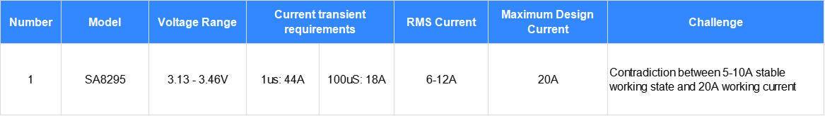
Table 1: SA8295 Power Supply Design Requirements
Note: The latest SA8295 design requirements are 21A (1 NPU) and 24A (2 NPUs), and this design can cover (30A overcurrent protection)
1.2 Design objectives
This design uses a LM25149 design domain controller first grade power supply, which can meet the requirements of transient current of 24A (100us) and meet the working requirements of steady-state operation of more than 10A, so as to achieve a comprehensive balance of volume, cost and performance.
Note: Transient current does not cause heat generation problem (for Qualcomm SA8295 only 100uS transient current), steady-state large current will cause an increase in temperature rise, the effect of temperature rise needs to be measured (design scheme is selected according to actual environmental conditions).
2- Schematic and PCB design
2.1 Core component selection
The criteria for the selection of domain controller primary switching power supply components: performance first, taking into account cost, and reducing the area of the PCB; Considering the EMC problem and current loop problem of BUCK switching power supply, it is in line with the general BUCK switching power supply design theory and rules, and the general design method can be referred to.
For details on electronic component selection and calculation, please refer to Chapter 1 (Decoding Qualcomm Automotive Domain Controller First-Stage Power Supply Design: Power Supply Design and Calculation)
Option 2 for this design (using eight 47uF C1210 packaged ceramic capacitors). The design is not limited to this selection, and the product design can be adjusted according to the actual situation, and the design optimization can be carried out according to the actual test results.
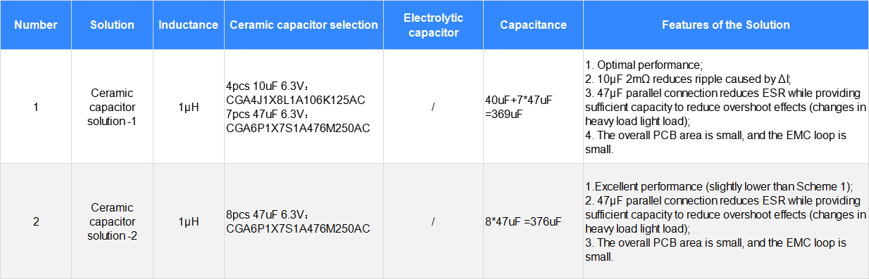
Table 2: BUCK power supply - scheme design
2.1.1 BUCK power supply-MOSFET selection
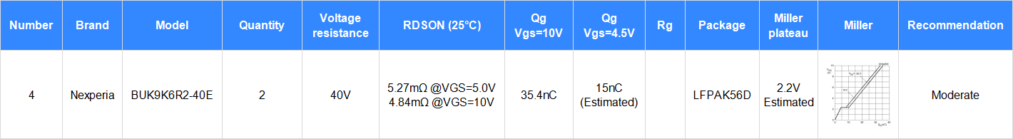
Table 3: BUCK power supply-MOSFET selection
2.1.2 BUCK power supply - inductor selection
Inductor selection adopts model: VSEB0660-1R0MV
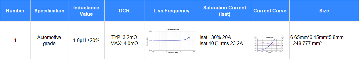
Table 4: Inductor Selection
2.1.3 Selection of output filter capacitor for BUCK power supply
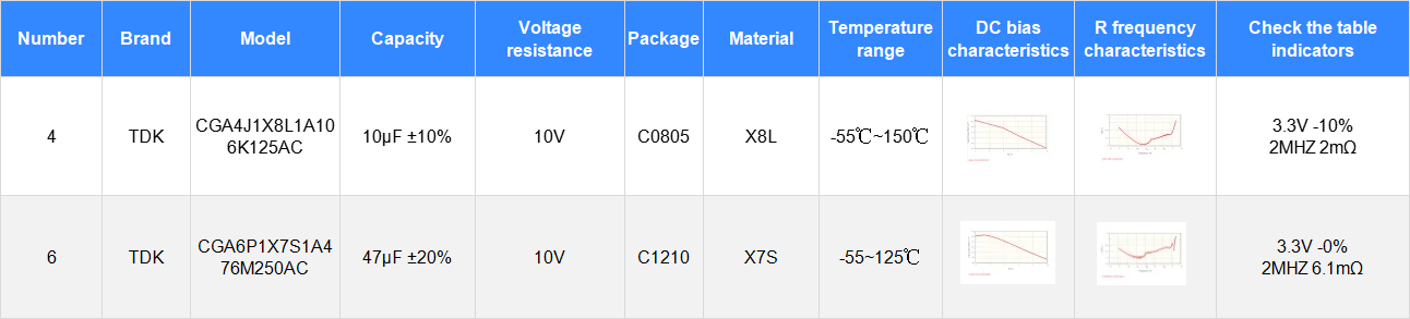
Table 5: Selection of output filter capacitor for BUCK power supply
2.1.4 BUCK power supply - selection of input filter capacitors
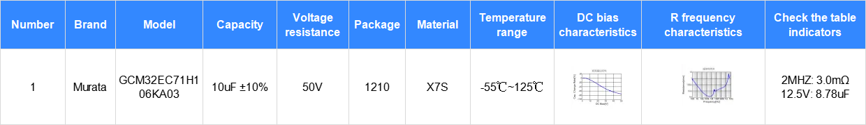
Table 6: BUCK power supply-input filter capacitor selection
2.2 Schematic and PCB design tools design
2.2.1 Schematic and PCB design: JLC Technology EDA (https://lceda.cn/)

Figure 1 Introduction to Caritron EDA
JLC Technology EDA is the leading free EDA development tool in China, with powerful functions and high development efficiency, this design adopts JLC Technology EDA design schematic diagram and PCB.
2.3 BUCK power supply-schematic design
2.3.1 BUCK power supply-schematic design
The principle design refers to the LM25149-Q1 specification and the official development board, and the design meets the basic theory of BUCK switching power supply and the design requirements of the primary power supply of high-pass domain controllers.
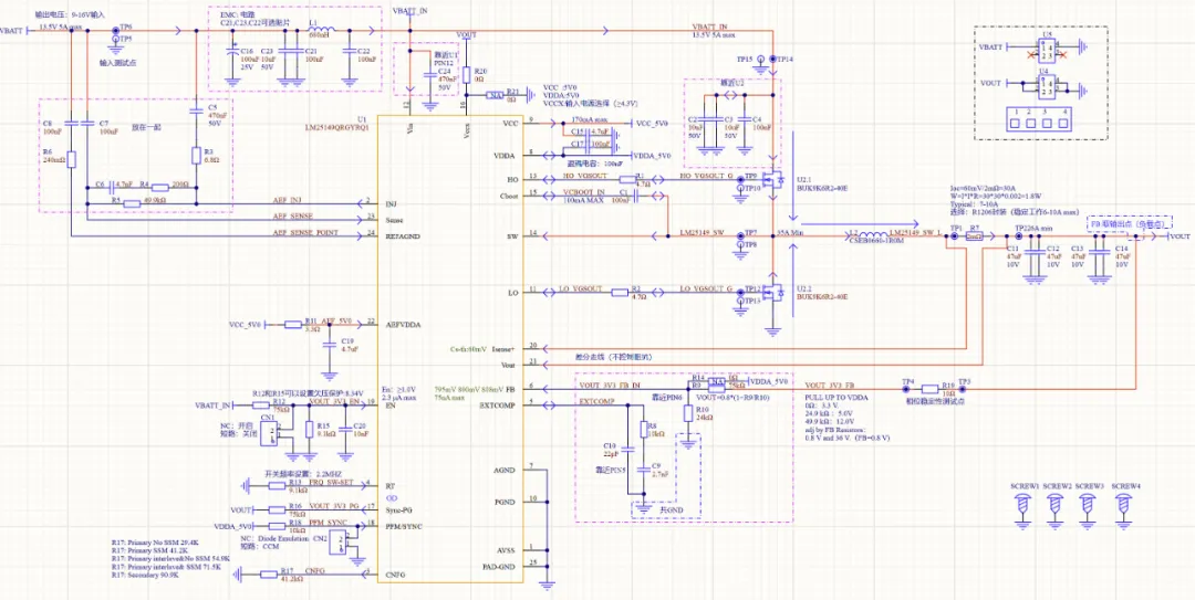
Figure 2 Schematic diagram of LM25149
2.3.2 BUCK Power Supply - key technology in schematic design
Input EMC circuit:
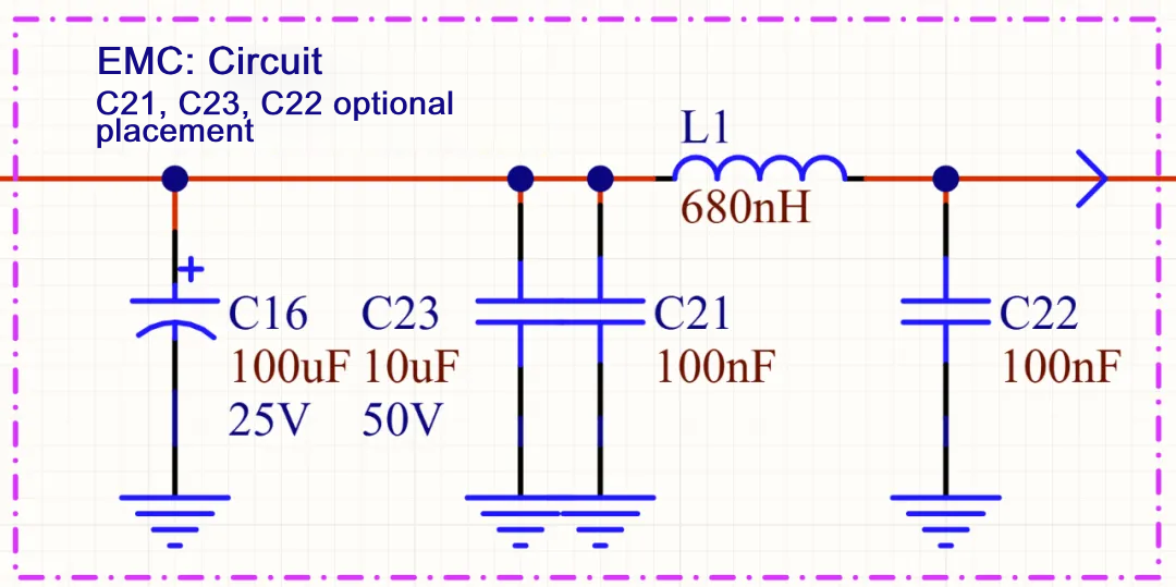
Technical points:
① The main function of L1 is to reduce the impact of conducted radiated noise from the switching power supply on the input power supply, the switching frequency of the switching power supply is 2.2MHz, L1 and C23 form an LC filter circuit (C16 is the electrolytic capacitor, mainly low frequencies below 500KHz), and 2.2MHz reduces by 60dB.
② C21 reduces switching noise (power tube rising edge and falling edge ringing), mainly reducing EMC noise from 10-100MHz.
③ If C21 and C23 are used in first-grade power supplies (before protection), you need to choose the flexible terminal capacitor model, and if it is protected, you can choose the automotive grade capacitor. A similar protection mechanism can also be implemented using two capacitors in series layout.
The same requirements are required for power MOSFETs and LM25149 input capacitors decoupling capacitors, this design is not used for performance verification, using a single ceramic, and the product-level design follows the automotive-grade design requirements.
Note: LM25419 active EMC cancellation and dual random spread spectrum technology, only to a certain extent the EMC amplitude is reduced, and EMC can not be eliminated, for the switching frequency of 2.2MHz related energy, high current (≥10A) above the application still has the risk of exceeding the standard, to the actual debugging shall prevail, if the removal of C23 can still be through conducted radiation, it can save the application of C23 and reduce the cost.
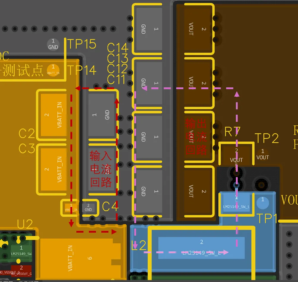
BUCK power input capacitors:
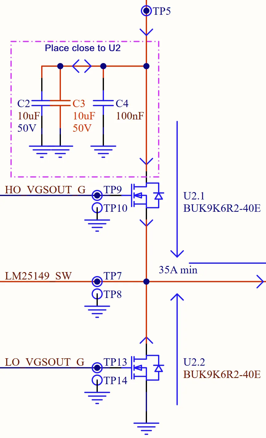
① C2, C3 are BUCK power input capacitors, which are crucial for the performance of switching power supply EMC, 10uF capacitors choose impedance around 2Mhz ≤5mΩ, CGA4J1X8L1A106K125AC and CGA6P1X7S1A476M250AC have good technical indicators for reference, capacitor selection can choose X7R, 35V/50V withstand voltage, package C1210 and C1206 are available. The C1210 package is selected for this design, which allows for a wide range of model verification performance.
② C4 is a high-frequency switching EMC capacitor, choose 50V X7R, C0402 package.
C2, C3, C4, Layout need to pay attention to the current loop (refer to the details of Layout), meet the basic BUCK power input capacitance requirements and design theory, you can learn the BUCK switching power supply theory to deepen the understanding of input capacitor.
③ TP7, TP9, TP13 are used to test the TG, BG and SW signals of the switch, and are used to test the reasonableness of the dead zone time, ringing performance, and the rising and falling edge performance of the MOSFET, which is an important electrical performance test index of the switching power supply.
The TP test point of GND is used to reduce the oscilloscope test GND loop and improve the test accuracy, and the LAYOUT needs to consider placing the test point as close to the relevant test signal as possible.
MOSFET gate drive resistor:
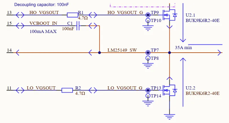
① R1 and R2 are the gate drive resistors of the MOSFET, which have an important impact on the rising and falling edges of the power MOSFET.
② The selection of R1 and R2 is affected by the combined reasons of the controlled BUCK power controller output current (controller (PULL and PUSH resistance), gate impedance and charge characteristics of the power MOSFET (input capacitance CISS), and the total resistance of the entire resistance is selected ≤ 10 ohms in the initial design, which also depends on the charge characteristics, and needs to be fine-tuned to select the appropriate resistance value.
③ R1 and R2 are also the key parameters that affect the switching noise EMC the most, and the core circuit factors that affect the switching loss.
Note: 6 test points are used to test switch characteristics and dead time.
Output power loop:
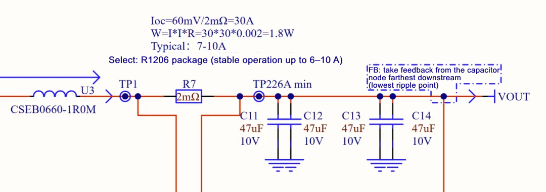
① Inductor selection: Inductor selection mainly considers two factors:
-Transient Working Current: Capable of transient output 24A (time: 100us);
-Steady-state working current: 10A, which can work stably at 10A current (covering 85℃ ambient temperature conditions);
-The transient operating current duration is ≤ 100us, and it occurs during the start-up phase, and only the condition of ensuring the inductance is unsaturated can meet the requirements (meeting the inductance value of the current).
② Selection of sampling resistor: The sampling resistor is selected in R1206 package, and the heat dissipation power ≥ 0.5W;
③ Selection of capacitors: Reference: Output filter capacitor chapter in the first part of the chapter;
Feedback Circuit:
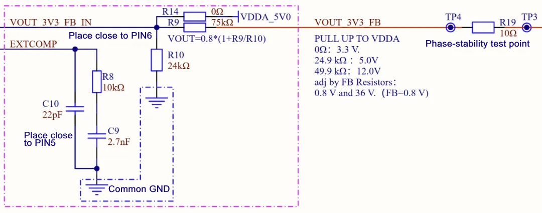
LM25149 has fixed output configuration and feedback output configuration, and the detailed content refers to the specification book;
① R14l connected to VDDA, output 3.3V
② R14=24.9K, output 5.0V
③ R14=49.9K, output 12.0V
Output voltage is configured with R14, R9 and R10 on the blank sticker;
R19 and reserved TP3, TP4: for testing, phase margin, traverse frequency, etc.
Note: TP3 and TP4 are used to test phase margin, traverse frequency, etc.
Function Settings:
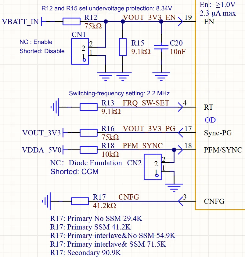
① EN: enable signal, turn on the power ≥ 1.0V, can be protected by precision undervoltage;
② Sync-PG: Synchronous output or Power good, this design is for Power Good;
③ PFM/SYNC
-Default (NC) jumper: Diode analogue, small current output, can work at high efficiency;
-Short circuit jumper to GND, forced CCM mode;
④ Chip working mode setting: a total of 5 working modes (refer to the specification book).
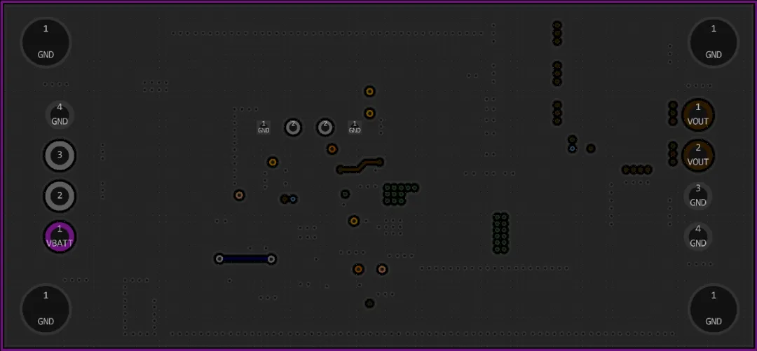
2.4 BUCK power supply-PCB design
2.4.1 BUCK power supply-PCB design
① -TOP
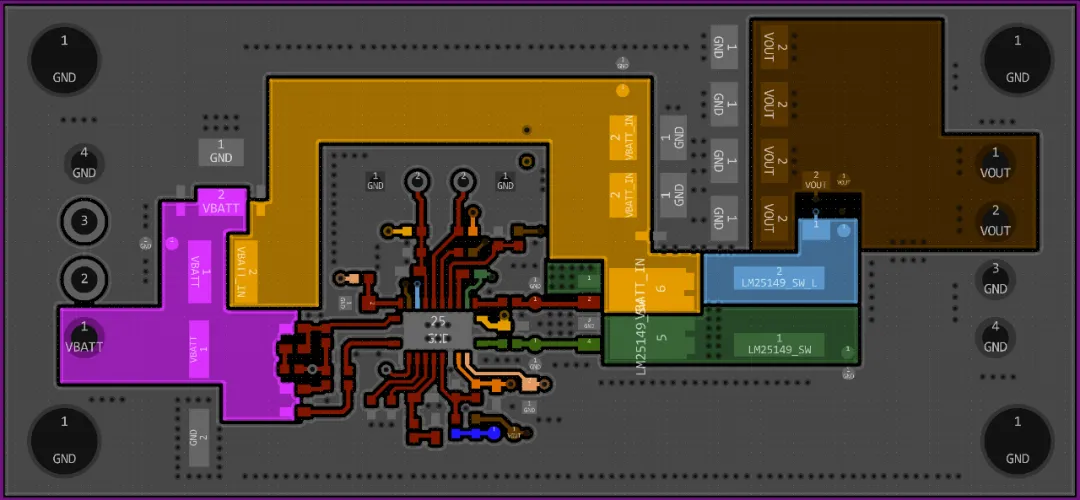
② -GND
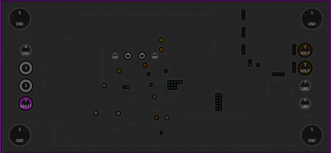
③ -Signal
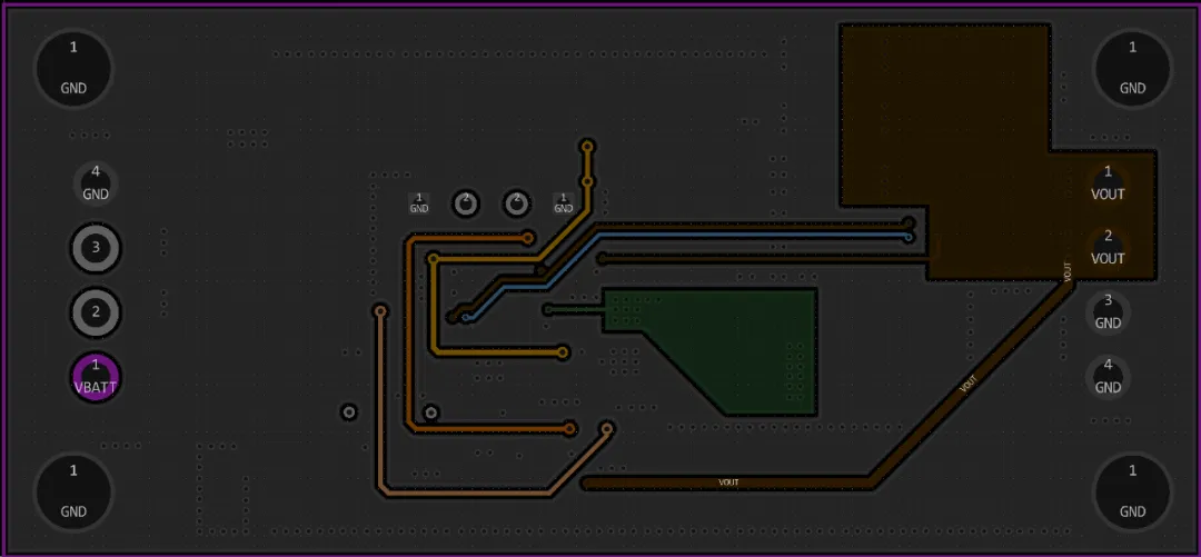
④ -Bottom
2.4.2 BUCK power supply-key technology for PCB design
Input and output capacitor loops:
① The input and output capacitors of BUCK power supply maintain a minimum loop, which has an important impact on EMC;
② C4 is mainly used to absorb the ringing noise of the rising and falling edges of the switch.
MOSFETs and Inductor Loops:
① The use of two-in-one MOSFETs reduces the layout area and costs, and the disadvantage is that the Layout SW cannot maintain the minimum loop;
② The SW point of the 2-in-1 MOSFET cannot realize the same layer of PCB traceability, and the layer laying surface needs to be changed to achieve continuous power current.
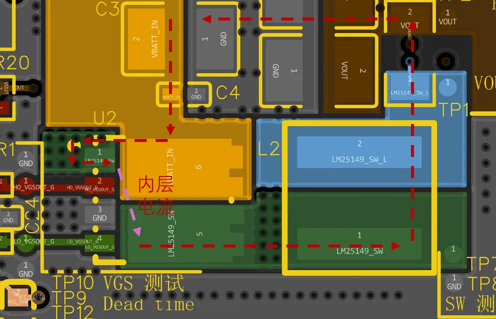
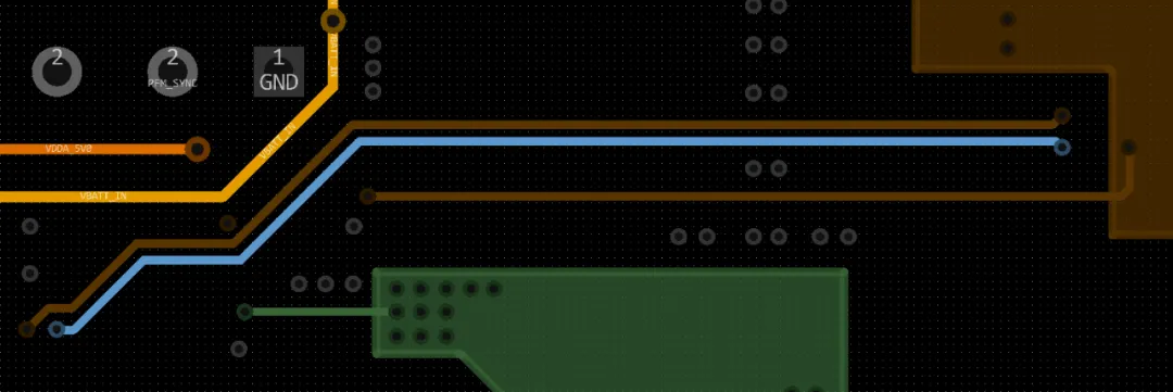
Sampling current:
① The sampling current needs to be differential traces, and there needs to be a reference GND plane;
② There is no need to control impedance and equal length, and the traces maintain the minimum spacing of the layout.
FB Feedback:
Resistors and other devices are close to the control chip pins.
Heat dissipation and GND:
Heating devices: MOSFETs, inductors, and sampling resistors can appropriately increase the heat conduction in the plane area, and increasing the GND vias can help improve the heat dissipation conditions of the whole board.
3- Domain-controlled first-grade BUCK power supply design - summary
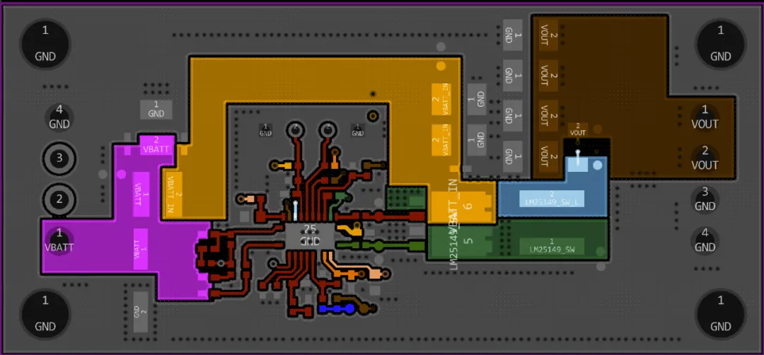
3.1 3D Drawing
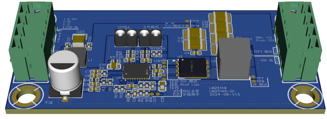
3D Figure-1
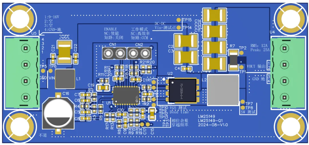
3D Figure-2
3.2 Design Summary
① The switching power supply design adopts a 4-layer design, PCB thickness 1.6mm, size 30X65mm;
② The output current can meet the maximum transient current of Qualcomm SA8295 of 24A, and supports steady-state output capability of more than 10A.
4- About Codaca Electronics
Codaca focuses on independent R&D, design and manufacturing of inductors, and the VSEB0660-1R0M is suitable for the development and application of Qualcomm platforms. It has technical advantages such as high cost performance, strong anti-saturation current ability, and low heat generation, and has an industry-leading power-to-volume ratio. Codaca focuses on technology research and development, technological innovation, develops excellent products for the inductor industry, and helps the development and application of electronic products..
5- Test and Verification
For subsequent testing and verification, please refer to: 03- Decoding Qualcomm Automotive Domain Controller First-Stage Power Supply Design: Performance Test Measurement Analysis.
[Reference]
1.LM25149-Q1:ti.com.cn/product/cn/LM25149-Q1
2.BUK9K6R2-40E:https://www.nexperia.cn/product/BUK9K6R2-40E